im trying to get the fan working on my Ms1 v2.2 board, and am having some trouble, so here is what ive done
-built the transistor circuit on a piece of protoboard, double checking that looks ok
- pulled ground from unbanded side of D1, and + from banded side of d9
-ran output to x12 which should correspond to pin 27
Where do i pull the signal from that goes onto the resistor on the proto board? does the v2.2 board have a JSO area? if not then where do i get the signal from?
Mike
Fan info
Moderators: jsmcortina, muythaibxr
-
Matt Cramer
- Super MS/Extra'er
- Posts: 17507
- Joined: Thu Apr 16, 2009 8:08 pm
Re: Fan info
Valid possible sources include:
X2 - dedicated fan control setting
X4 - output 1
X5 - output 2
Top of R14 with R14 removed - output 3
X2 - dedicated fan control setting
X4 - output 1
X5 - output 2
Top of R14 with R14 removed - output 3
Matt Cramer -1966 Dodge Dart slant six running on MS3X
-
MikeDTuned
- MS/Extra Newbie
- Posts: 29
- Joined: Thu Jun 26, 2014 5:49 pm
Re: Fan info
Thanks for the help! is there any special setup when doing fan control besides setting x2 to fan control, (under output pin options and adjusting temps under output pin settings?
-
Matt Cramer
- Super MS/Extra'er
- Posts: 17507
- Joined: Thu Apr 16, 2009 8:08 pm
-
MikeDTuned
- MS/Extra Newbie
- Posts: 29
- Joined: Thu Jun 26, 2014 5:49 pm
Re: Fan info
One last check, just to cover my bases,
in this diagram, the transisor ends are labled "1,2 & 3"
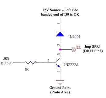
However in all the diagrams of the pn2222a transisor, things are labled "E,B & C"
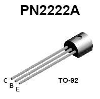
I went under the assumption that
1 = E
2 = B
3 = C
Is this correct?
in this diagram, the transisor ends are labled "1,2 & 3"
However in all the diagrams of the pn2222a transisor, things are labled "E,B & C"
I went under the assumption that
1 = E
2 = B
3 = C
Is this correct?
-
MikeDTuned
- MS/Extra Newbie
- Posts: 29
- Joined: Thu Jun 26, 2014 5:49 pm
Re: Fan info
got it working,, turns out i was wrong with the above asumption
for future reference The correct orientation is
1 = C
2 = B
3 = E
for future reference The correct orientation is
1 = C
2 = B
3 = E
-
slow_hemi6
- Super MS/Extra'er
- Posts: 4122
- Joined: Fri May 07, 2004 3:33 am
- Location: Australia
Re: Fan info
Collector, Base and Emitter are the correct terms. Their arrangement on the pins varies from transistor part No to transistor part No. The diagram for a NPN transistor never changes though so looking at the diagram the horizontal line that joins the vertical is always the Base, the line with outward arrow is always the Emitter and the top plain line is always the Collector.
So you can see what you have written there with relation to the MS diagram is wrong. 3 is collector and 1 is emitter.
Note the diagram and EBC orientation for PNP transistors is the same but the arrow on the emitter faces inwards.
So you can see what you have written there with relation to the MS diagram is wrong. 3 is collector and 1 is emitter.
Note the diagram and EBC orientation for PNP transistors is the same but the arrow on the emitter faces inwards.
Find the Manuals up top under Quick links: Manuals. 
Cheers Luke
Cheers Luke