Hi Ralf,
dougie2 wrote:
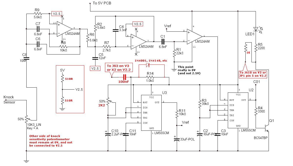
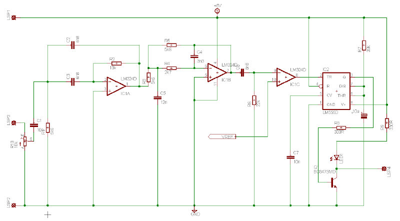
1. First of all your 100nF capacitor to Pin2 of U3 needs special attention! If the incoming tacho signal gets low, it generates a negative trigger signal at U3. The capacitor then gets charged to +5V. When then the tacho signal switches to 5V it boosts the voltage at the trigger input of the NE555 to 10V !! You need to put in a protection diode which limits the voltage at pin 2 to somewhat 5,7V, otherwise the NE555 might die.
There is such a protection diode on my board already. This was an omission I made from the schematic in error; the schematic in the link above has been corrected. Thank you for pointing it out. (I know only the foolish would leave these things down to the IC's internal ESD protection diode!)
2. The timing constant at U3 using the potetiometer and C10 is critical for the NE555 to discharge. At high revs the internal transistor of the NE555 has to discharge the 2,2uF quite often, which results in a high current. Better using a 470nF capacitor and a 10k or 50k potentiometer
I only changed the value of the potentiometer to 2K2 because I personally found that the ideal setting for me was somewhere around 1K5, and the 2K2 potentiometer made it easier to adjust. It's also a very bad thing for there to be no other series resistor in line with the potentiometer, for obvious reasons, and if I were drawing the schematic from scratch I'd have added that too. If I were doing this from scratch myself then it would have been different, but please remember that the capacitor value, lack of potentiometer series resistor, etc. are just as they were when presented by the OP. Really, I'm just trying to indicate on the schematic what changes I made to make the circuit *work*. But I agree it would be good to draw another shematic that incorporates all of these suggestions.
3. Both buffer capacitors connected to pin 5 of the NE555s need to be 100nF enspecially in noisy environment
3. Again, these values are from the OP's schematic.
4. 100nF capcitors and a 100uF electrolytic capacitor need to be installed across the supply voltage. In general it's not recommended using th bipolar version of the NE555 here... the cmos version e.g. TLC555 would work much better...
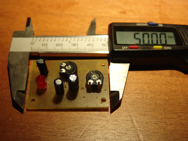
4. All three ICs on my board have tant and ceramic capacitors put directly across the power supply pins, on the bottom side of the board. And I am using CMOS 555 devices.
5. Your output will not work as intended. The voltage at the cathode of the LED will switch between 5V and 5V minus the forward voltage of the diode. In case of a red LED (Vf about 1,2V) it would only switch between 5V (high signal) and 3,8V (Low Signal). The 1k output resistor needs to be connected to the collector of Q1...
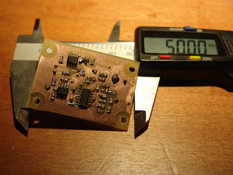
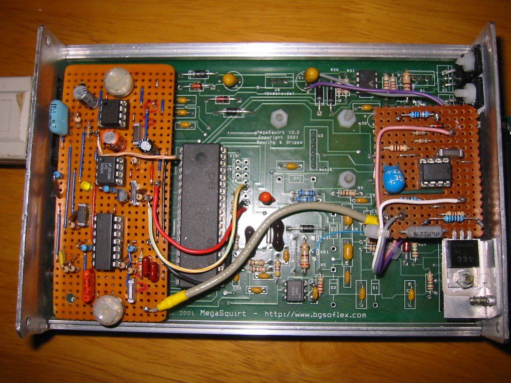
5. This is a mistake in my schematic for which I apologise - it was late last night and I did it in a hurry. It has now been amended in the link above. If you look closely enough at the photograph of my board, you can see the output clearly goes to the collector of Q1!
I do thank you for pointing out the two errors in my marked-up schematic (missing protection diode and output connection point) and it has now been amended.
Please consider that a lot of people are relying on the information provided here. So a lot of frustration would be caused when people try to make things work which cannot work.
Okay - I'm a bit suprised and upset about the last comment which suggests I could be posting something that cannot be made to work. Is this directed at the original poster and contributor of the design, or is it directed towards me? Because from my point of view, I have started out with a design that had fundamental design issues (such as trying to run those two filters from a single-rail supply as they were, and so forth) that simply could not be made to work at all. Indeed a lot of frustration WAS caused to me when I realised I had constructed something that simply could not work. So I went about applying a few changes, and I was rather pleased to have been able to make the HPF / LPF filters and 555 circuit work after all with a few very simple changes to my stripboard layout, and I didn't have to completely junk the design after all. So, I thought it would be helpful to present the findings to everyone else.
My aim was not to present an absolutely perfect schematic; I was merely just tring to show the important changes I made that made it actually
work.
Trev
PS. Out of interest, what design change did you implement for the filters?