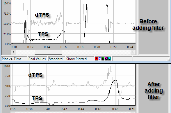
gslender wrote:I've updated a mod I released to include TPS oversampling such that it averages the results of many samples (~400) obtained inbetween the previous 50ms sample period. This has resulted in a significantly less noisy TPS signal, and to a degree, removed the need for any other type of TPS filtering.
If this much oversampling is needed to get the high degree of noise attenuation suggests that the noise signal at a much higher frequency than the original sampling rate. This suggests "spikey" type noise from switching edges (such as from injector drivers and coil drivers), contaminating the A/D inputs, from poor filtering, layout, grounding, or supply bypassing.
If the 400x oversampling is processor intensive then fixing the layout, adding a proper input filter, then doing only 4x oversampling (5 ms samples), and a 2-pole filter should get you the same noise-free signal without the processor burden.
I will point this out again:
It's from the last post on page 10:
http://www.msextra.com/forums/viewtopic ... &start=180
I totally hacked the PCB layout of my AEM ECU to get rid of the TPS noise.
In my AEM, I looked at the datasheet of the microcontroller whose A/D was doing the TPS.
What jumped out at me was this:
It cannot tolerate a voltage differential between the A/D input analog ground, and its main digital ground. And they have to be tied together.
And then, the AEM layout was divided into 3 ground plane areas:
- analog circuitry such as opamps, including the TPS input
- digital ground - uC was grounded here
- high current driver MOSFETs for injectors, etc
The 3 grounds were joined at a single 5V regulator for the whole board
This was one of the mistakes. This is commonly touted on the web and even appears in some databooks and
it is terrible advice. (Part of my day job is writing datasheets and Application Notes for mixed signal IC's, which have pins sensitive to 10 mV with 50 ns speeds and nearby pins which switch 500V and 10A in 30 ns). There should have been 3 separate 5V regulators for each section. Also the last bit of PCB connection from the analog ground area to said regulator ground pin, was long and skinny. This is mistake #2.
The sensor ground ECU pin was returned to the analog portion of the ground plane, and the high current driver MOSFET circuitry ground return was connected to the main power ground ECU pin.
Sounds correct, but it's not that simple.
The big problem was that the analog circuitry was sitting on a ground plane area that was a separate ground from the microcontroller ground, to which the A/D inputs are referenced. Any voltage appearing between the 2 grounds,
effectively appears on the A/D inputs. Why is there a voltage between them? 2 reasons:
1)
Signals going from the analog area to the microcontroller area or vice versa, will have a ground return path which is long and skinny, and this develops a voltage difference.
2) The loop that current from said signals has a large area which increases inductance which also develops a voltage difference for signals with fast dv/dt and di/dt.
The solution?
Join the analog and digital ground planes and turn them into a single effective ground plane, by jumpering across the gap between them, about an inch apart.
Then make sure that the engine sensors grounds are connected to the ECU sensor ground pin and connected to no other "grounds" in the car.
Peruse this website:
http://www.hottconsultants.com/techtips ... plane.html
Henry Ott wrote the reference book "Noise Reduction Techniques", and it was a course I taught for MSEE students and also for junior engineers where I worked.
From the site:

Some people suggest splitting the ground plane in order to isolate the digital ground currents from the analog ground currents. Although the split plane approach can be made to work, it has many potential problems especially in large complicated systems. Can you list some of these problems? One of the major ones is that you can not route a trace over the split in the plane (see Tech Tip Slots in Ground Planes). It is always better to have only a single reference plane for a system.
If you do split the ground plane and run traces across the split (left hand figure below), there will be no return path near the trace and the current will have to flow in a big loop. Current flowing in big loops produce radiation and high ground inductance. If you must split the ground plane and run traces across the split, you should do it as shown in the right hand figure below. By connecting the planes together at one point (a bridge) and routing all the traces so that they cross at this bridge point, you will have provided a return path for the current directly underneath each of the traces (hence a very small loop area).
The AEM PCB layout violated this rule in abundance. (Left half of above diagram).
A PCB with a single ground plane, partitioned into analog and digital sections, and discipline in routing the signals can usually solve an otherwise difficult layout problem, without creating the additional problems caused by a split ground plane. If the layout is done properly, the digital ground currents will remain in the digital section of the board and will not interfere with the analog signals. The routing, however, must be checked carefully to assure that the above mentioned routing restrictions are adhered to one hundred percent! The key to a successful mixed signal PCB layout, therefore, is proper partitioning and routing discipline, not a split ground plane.
If you are still skeptical about using a single ground plane on your mixed signal boards I suggest you do the following experiment. Layout the board with a split ground plane, but provide means for connecting the two planes together every 1/2 inch with jumpers or zero ohm resistors. Route the board properly, with no digital traces (on any layer) over the analog plane and no analog traces (on any layer) over the digital plane. Build the board and test it's functionality and EMC performance. Connect the planes together and test the board again for functionality and EMC performance. I think that you will find that in almost all cases, both the functional performance and the EMC performance of the board will be better with the single ground plane.
This jumpering is effectively what I did with my AEM.
The improvement from shorting the polyfuse in the MS possibly points to a similar layout problem.
The remaining noise is probably due to the layout.
If someone can provide a link to the PCB layout, I could take a look at it.